Mobile Supported Video

  • Subscribe to our RSS feed.
  • Twitter
  • StumbleUpon
  • Reddit
  • Facebook
  • Digg

Tuesday, 5 November 2013

Synaptic Transistor Learns While It Computes

Posted on 01:03 by Unknown
Our brains have upwards of 86 billion neurons, connected by synapses that not only complete myriad logic circuits; they continuously adapt to stimuli, strengthening some connections while weakening others. We call that process learning, and it enables the kind of rapid, highly efficient computational processes that put Siri and Blue Gene to shame.
Materials scientists at the Harvard School of Engineering and Applied Sciences (SEAS) have now created a new type of transistor that mimics the behavior of a synapse. The novel device simultaneously modulates the flow of information in a circuit and physically adapts to changing signals.

Exploiting unusual properties in modern materials, the synaptic transistor could mark the beginning of a new kind of artificial intelligence: one embedded not in smart algorithms but in the very architecture of a computer. The findings appear in Nature Communications.

"There's extraordinary interest in building energy-efficient electronics these days," says principal investigator Shriram Ramanathan, associate professor of materials science at Harvard SEAS. "Historically, people have been focused on speed, but with speed comes the penalty of power dissipation. With electronics becoming more and more powerful and ubiquitous, you could have a huge impact by cutting down the amount of energy they consume."

The human mind, for all its phenomenal computing power, runs on roughly 20 Watts of energy (less than a household light bulb), so it offers a natural model for engineers.
"The transistor we've demonstrated is really an analog to the synapse in our brains," says co-lead author Jian Shi, a postdoctoral fellow at SEAS. "Each time a neuron initiates an action and another neuron reacts, the synapse between them increases the strength of its connection. And the faster the neurons spike each time, the stronger the synaptic connection. Essentially, it memorizes the action between the neurons."

In principle, a system integrating millions of tiny synaptic transistors and neuron terminals could take parallel computing into a new era of ultra-efficient high performance.
While calcium ions and receptors effect a change in a biological synapse, the artificial version achieves the same plasticity with oxygen ions. When a voltage is applied, these ions slip in and out of the crystal lattice of a very thin (80-nanometer) film of samarium nickelate, which acts as the synapse channel between two platinum "axon" and "dendrite" terminals. The varying concentration of ions in the nickelate raises or lowers its conductance — that is, its ability to carry information on an electrical current — and, just as in a natural synapse, the strength of the connection depends on the time delay in the electrical signal.

Structurally, the device consists of the nickelate semiconductor sandwiched between two platinum electrodes and adjacent to a small pocket of ionic liquid. An external circuit multiplexer converts the time delay into a magnitude of voltage which it applies to the ionic liquid, creating an electric field that either drives ions into the nickelate or removes them. The entire device, just a few hundred microns long, is embedded in a silicon chip.
The synaptic transistor offers several immediate advantages over traditional silicon transistors. For a start, it is not restricted to the binary system of ones and zeros.
Read More
Posted in | No comments

Tuesday, 20 March 2012

Holey Optochip First to Transfer One Trillion Bits of Information per Second Using the Power of Light developed by IBM

Posted on 01:46 by Unknown

IBM scientists today reported of a prototype optical chipset, dubbed “Holey Optochip”, that is the first parallel optical transceiver to transfer one trillion bits – one terabit – of information per second, the equivalent of downloading 500 high definition movies. The report will be presented at the Optical Fiber Communication Conference taking place in Los Angeles.
With the ability to move information at blazing speeds – eight times faster than parallel optical components available today – the breakthrough could transform how data is accessed, shared and used for a new era of communications, computing and entertainment. The raw speed of one transceiver is equivalent to the bandwidth consumed by 100,000 users at today’s typical 10 Mb/s high-speed internet access. Or, it would take just around an hour to transfer the entire U.S. Library of Congress web archive through the transceiver.  
Progress in optical communications is being driven by an explosion of new applications and services as the amount of data being created and transmitted over corporate and consumer networks continues to grow. At one terabit per second, IBM’s latest advance in optical chip technology provides unprecedented amounts of bandwidth that could one day ship loads of data such as posts to social media sites, digital pictures and videos posted online, sensors used to gather climate information, and transaction records of online purchases.  
“Reaching the one trillion bit per second mark with the Holey Optochip marks IBM’s latest milestone to develop chip-scale transceivers that can handle the volume of traffic in the era of big data,” said IBM Researcher Clint Schow, part of the team that built the prototype. “We have been actively pursuing higher levels of integration, power efficiency and performance for all the optical components through packaging and circuit innovations. We aim to improve on the technology for commercialization in the next decade with the collaboration of manufacturing partners.”  
Optical networking offers the potential to significantly improve data transfer rates by speeding the flow of data using light pulses, instead of sending electrons over wires. Because of this, researchers have been looking for ways to make use of optical signals within standard low-cost, high-volume chip manufacturing techniques for widespread use. 
Holey Optochip
Photomicrograph of IBM Holey Optochip. Original chip dimensions are 5.2 mm x 5 .8 mm.
Using a novel approach, scientists in IBM labs developed the Holey Optochip by fabricating 48 holes through a standard silicon CMOS chip. The holes allow optical access through the back of the chip to 24 receiver and 24 transmitter channels to produce an ultra-compact, high-performing and power-efficient optical module capable of record setting data transfer rates. 
The compactness and capacity of optical communication has become indispensable in the design of large data-handling systems. With that in mind, the Holey Optochip module is constructed with components that are commercially available today, providing the possibility to manufacture at economies of scale. 
Consistent with green computing initiatives, the Holey Optochip achieves record speed at a power efficiency (the amount of power required to transmit a bit of information) that is among the best ever reported. The transceiver consumes less than five watts; the power consumed by a 100W light bulb could power 20 transceivers. This progress in power efficient interconnects is necessary to allow companies who adopt high-performance computing to manage their energy load while performing powerful applications such as analytics, data modeling and forecasting. 
By demonstrating unparalleled levels of performance, the Holey Optochip illustrates that high-speed, low-power interconnects are feasible in the near term and optical is the only transmission medium that can stay ahead of the accelerating global demand for broadband. The future of computing will rely heavily on optical chip technology to facilitate the growth of big data and cloud computing and the drive for next-generation data center applications.
Technical Aspects of the Holey Optochip
Back of Holey Optochip
Photomicrograph of the back of the IBM Holey Optochip with lasers and photodectors visible through substrate holes.  
Parallel optics is a fiber optic technology primarily targeted for high-data, short-reach multimode fiber systems that are typically less than 150 meters. Parallel optics differs from traditional duplex fiber optic serial communication in that data is simultaneously transmitted and received over multiple optical fibers. 
A single 90-nanometer IBM CMOS transceiver IC with 24 receiver and 24 transmitter circuits becomes a Holey Optochip with the fabrication of forty-eight through-silicon holes, or “optical vias” – one for each transmitter and receiver channel. Simple post-processing on completed CMOS wafers with all devices and standard wiring levels results in an entire wafer populated with Holey Optochips. The transceiver chip measures only 5.2 mm x 5.8 mm. Twenty-four channel, industry-standard 850-nm VCSEL (vertical cavity surface emitting laser) and photodiode arrays are directly flip-chip soldered to the Optochip. This direct packaging produces high-performance, chip-scale optical engines. The Holey Optochips are designed for direct coupling to a standard 48-channel multimode fiber array through an efficient microlens optical system that can be assembled with conventional high-volume packaging tools. 
Read More
Posted in | No comments

Tuesday, 21 February 2012

Fully Laser Integrated Photonics (FLIP) - A revolution in Computing Technology on the edge

Posted on 00:19 by Unknown
Fully Laser Integrated Photonics (FLIP) may replace conventional electronics in a whole lot of computing and cut down computing's ever-rising demand for power (Google today already accounts for 1% of US power consumption) by an order of magnitude. 

It is as fast as lightning, it is cool, it is going to change the world as fundamentally as did manned flight and it has been created by an Indian, Raj Dutt... Okay, Stanford, Massachusetts Institute of Technology and the US Navy chipped in. 

FLIP has been enabled by a breakthrough in the science of materials just announced in the US: Indian American scientist and entrepreneur Dr Birendra (Raj) Dutt along with a top team of researchers at his own company APIC Corporation, the Massachusetts Institute of Technology and Stanford University has discovered how to make germanium produce a laser when charged with electricity. This would eventually allow a new breed of microchips to be built on a commercial scale in which pulses of light, called photons, zip at top speed along nano-sized waveguides of the self-same germanium etched into silicon, instead of electrons whizzing around in copper circuits on silicon as in today's chips. 

When electrons move through a conductor, they produce heat, which then has to be removed using additional energy. Photons, on the other hand, do not produce heat as they move through their waveguides at the speed of light, hence no energy is required to cool photonic chips. Further, use of doped germanium together with the straining of this material when grown on silicon produces a laser that makes mass commercial production of photonic chips possible. 


Germanium belongs to the same group of elements as silicon, making full integration of laser chips possible. While use of photons in chips is not new, till the present discovery of making germanium 'lase', it had not been possible to have integrated photon chips. Dr Dutt, an IIT-Kharagpur, aeronautical engineering alumnus of the class of 1971, founded APIC Corporation in 1999 for research, development and production of highly integrated photonic and electronic technology. Today his company has forged strategic relationships with a large number of universities and institutions in the US. It has a wholly-owned fabrication facility in Honolulu. The breakthrough research, which was achieved under a US government contract, was sponsored by the Naval Air Systems Command, Aircraft Division,(NAVAIR) and the National Security Agency (NSA) and funded by the US department of defence. 


Dr Dutt, founder and chief technology officer of APIC and the principal investigator on this project, along with his co-investigator, Dr Jurgen Michel, senior research scientist at Massachusetts Institute of Technology, succeeded in getting germanium, which is a group IV material that is silicon CMOS compatible, to lase when electrically pumped."Both the scientific community and industry have been waiting for a breakthrough like this. The new photonic chips will have exponentially better performance at a tiny fraction of current power usage, and a tremendous positive impact on the environment through drastic reduction of heat generated by computing devices," Dr Dutt told ET from his office in Culver City, California. 

Experts in the US are upbeat about APIC's research. Dr. Tony Tether, former director of Defence Advanced Projects Research Agency (DARPA), the US agency responsible for development of new technology for use by the military has stated that, "The APIC FLIP effort has achieved creating a germanium LASER heretofore thought to be impossible. Take these results as the Kitty Hawk demonstration where it was shown that manned flight was possible." 

APIC now plans to commercially roll-out the fully manufacturable prototype of the photonic chip over the next 18-24 months and has teamed up with R&D fabrication facility at the College of Nanoscale Science and Engineering at the University of Albany in New York state. "The performance increase comes with a stunning decrease in the amount of power needed as compared to today's chips. Voracious demand for online and mobile services, along with cloud computing, has caused explosive growth in the amount of data centres and the energy they gobble up. But photons simply require much less power than electrons to propel, and most importantly they do not generate heat. Using photonic processors and components would enable massive energy savings for data centres, which would consume only about 10% of today," Dr Dutt added. 

Once the chip has been commercially launched, APIC Corporation could look at tie-ups with other chip makers for production. The company, which is a US government contractor, owns the patent for the photon chip technology and Dr Dutt believes that there could be opportunities in the future to look at tie-ups with institutions in India for making the photon-chip.
Read More
Posted in | No comments

Monday, 6 February 2012

Bamboo-inspired Plantbook concept powered by self-generated hydrogen

Posted on 04:46 by Unknown
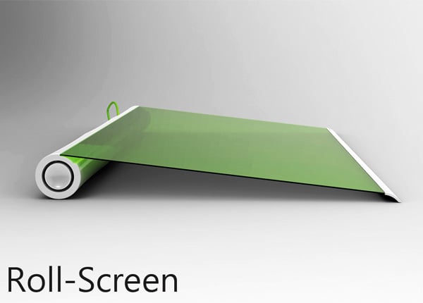
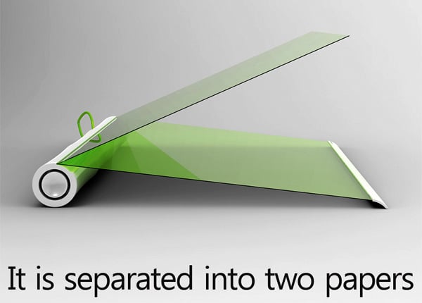
The Plantbook or the 'oxygenated notebook', a concept designed by Seunggi Baek and Hyerim Kim, is a laptop whose technology is largely inspired by the bamboo plant that derives its nutrients when soaked in water. The design of Plantbook is amazing and unique. It comprises of a cylindrical structure with two rollout screens (for the keyboard and monitor). The green color of the notebook is a representation of its 'green' capabilities. There is no need for you to charge the notebook as it uses hydrogen generated by electrolysis of water as its energy source.
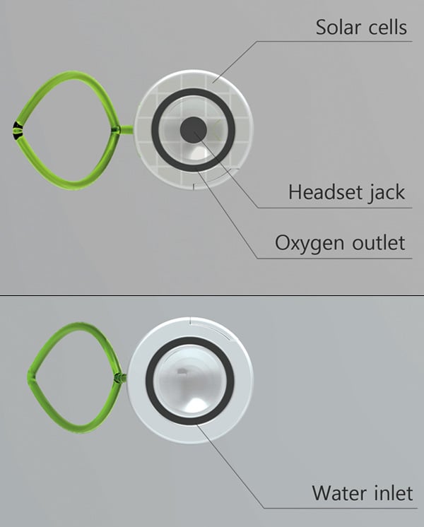
The Plantbook when rolled back into its cylindrical form gets placed inside a beaker full of water to soak it, thus generating hydrogen via the process of electrolysis and releasing oxygen. The energy required for electrolysis is provided by a solar heat plate that is affixed at the top of the device. Much like a plant, the Plantbook produces energy releases oxygen. Furthermore, the Plantbook has a strap or a hand ring affixed to the top that has a leaf-like shape with green LED; it indicates the extent to which the battery has been charged. It is incredible to see how much energy we can generate through natural means - without having to cut down trees, eat into our limited oil and coal reserves, etc. 
The Plantbook definitely seems to be a path-breaking concept.


Read More
Posted in | No comments

Friday, 13 January 2012

IBM developing new, tiny storage device of just 12 atoms

Posted on 01:43 by Unknown
SAN JOSE, Calif. — Researchers at I.B.M. have stored and retrieved digital 1s and 0s from an array of just 12 atoms, pushing the boundaries of the magnetic storage of information to the edge of what is possible.
The findings, being reported Thursday in the journal Science, could help lead to a new class of nanomaterials for a generation of memory chips and disk drives that will not only have greater capabilities than the current silicon-based computers but will consume significantly less power. And they may offer a new direction for research in quantum computing.
“Magnetic materials are extremely useful and strategically important to many major economies, but there aren’t that many of them,” said Shan X. Wang, director of the Center for Magnetic Nanotechnology at Stanford University. “To make a brand new material is very intriguing and scientifically very important.”
Until now, the most advanced magnetic storage systems have needed about one million atoms to store a digital 1 or 0. The new achievement is the product of a heated international race between elite physics laboratories to explore the properties of magnetic materials at a far smaller scale.
Last May, a group at the Institute of Applied Physics at the University of Hamburg in Germany reported on the ability to perform computer logic operations on an atomic level.
The group at I.B.M.’s Almaden Research Center here, led by Andreas Heinrich, has now created the smallest possible unit of magnetic storage by painstakingly arranging two rows of six iron atoms on a surface of copper nitride.
Such closeness is possible because the cluster of atoms is antiferromagnetic — a rare quality in which each atom in the array has an opposed magnetic orientation. (In common ferromagnetic materials like iron, nickel and cobalt, the atoms are magnetically aligned.)
Under the laboratory’s founder, Don Eigler, I.B.M. has explored the science of nanomaterials far smaller than the silicon chips used in today’s semiconductors. Dr. Eigler recently retired from the company but is a co-author of the Science paper.
The researchers now use a scanning tunneling microscope, which looks like a giant washing machine festooned with aluminum foil, not only to capture images of atoms but to reposition individual atoms — much the way a billiard ball might be moved by a pool cue with a sticky tip.
Although the research took place at a temperature near absolute zero, the scientists wrote that the same experiment could be done at room temperature with as few as 150 atoms.
As part of its demonstration of the antiferromagnetic storage effect, the researchers created a computer byte, or character, out of an individually placed array of 96 atoms. They then used the array to encode the I.B.M. motto “Think” by repeatedly programming the memory block to store representations of its five letters.
Moreover, Dr. Heinrich said, smaller groups of atoms begin to exhibit quantum mechanical behavior — simultaneously existing in both “spin” states, in effect 1 and 0 at the same time.
In theory, such atoms could be assembled into Qbits — the basic unit of an experimental approach to computing that might one day exceed the capabilities of today’s most powerful supercomputers.
“If you do this with two atoms, then they behave more like a quantum mechanical object,” Dr. Heinrich said. “This is why science is interested in this work more than the technology.”
In an interview in a small laboratory office here, he said he was planning to knock out a wall to create room for an expanded effort in exploring the quantum mechanical properties of the antiferromagnetic effect.
“This is really where we live,” he said. “If you step outside of the press release, we are trying to control the quantum mechanics of this spin behavior to coax them to do whatever we want them to do.”
Computer industry analysts said the I.B.M. effort heralded a new direction for nanotechnology and that it might offer a route to new kinds of nanomaterials.
“Nanotechnology labs are going to begin asking, ‘What else is going on down there?’ ” said Richard Doherty an electrophysicist who is director of Envisioneering, an industry consulting firm based in Seaford, N.Y. “The information storage side of this is fantastic, but this truly changes our ideas of the behavior of materials at molecular levels.”
Antiferromagnetic materials are now instrumental in two types of data storage products. They are essential for the manufacture of recording heads, which resemble phonograph needles and are used in today’s hard disk drives. They are also used in a new type of memory chip known as spin-transfer-torque RAM, or STT-RAM, which some view as a future competitor for DRAM and Flash memory chips.
Dr. Heinrich said that the tiny devices built with scanning tunneling microscopes would never be more than laboratory experiments.
However, he noted that many research groups are exploring ways of designing novel materials using self-assembly methods, including mechanical and biological approaches.
Industry executives said that as the semiconductor industry draws closer to exhausting the ability to scale down today’s circuits using lithographic tools that etch patterns on the surface of silicon wafers, an intense international hunt is under way for a manufacturing technology beyond microelectronics.
“The nation that discovers the next logic switch will lead the nanoelectronics era and reap the economic rewards associated with it,” said Ian Steff, vice president for global policy and technology partnerships of the Semiconductor Industry Association.
Read More
Posted in | No comments

Monday, 17 October 2011

Kingmax introduces first-in-class 1TB SSDs and Nano Gaming RAM worldwide and in Indian channel partners

Posted on 06:38 by Unknown

Kingmax, a Taiwanese company best known for its DRAM and NAND Flash memory, heralded its first major push into the Indian market last week, introducing its partners in the country, as well as some its latest products, including first-in-class 1TB SSD drives and 64GB SDXC cards.
The company announced its four major distribution partners - Salora, Kingstar, Redington & Supertron – at the channel partner and media event. Also at hand, was Mr. Lawrence Chang, Kingmax’s Global Sales VP, who introduced the Kingmax group of companies, and spoke about the future of NAND Flash and DRAM memory, as well as SSDs and their impact on cloud computing.
Kingmax’s latest achievement – a first-in-class 1TB SSD drive – was shown off at the event, and is due to hit retail availability son. The company, which claims it has a technological advantage with its own semi-conductor assembly and testing subsidiary – Kingmax Semiconductor – was able to develop the 1TB 2.5-inch SATA II SSDs with its patented 8 stacked die process.

Kingmax also highlighted its globally well-received Nano Gaming RAM at the event, also due for retail availability soon. It is known as the first 2400MHz DDR3 performance module that doesn’t require an integrated or after market heatsink to operate, and yet returns relatively cooler temperatures, even under the stress of overclocking.The new family of SSDs stretches from 32GB all the way to 1TB, and you can check out the performance figures below. So far, pricing details have not yet been revealed. Kingmax also revealed it intends to launch 2TB 2.5-inch SSDs by Q1 2012, preceded by SATA III 1TB SSDs.
Kingmax says it managed this by adding diamond-like carbon (DLC) and silicon in the wafer, allowing for what it calls Nano Thermal Dissipation Technology (NTDT), which by acting like a permeable membrane also assists in cabinet airflow. The Nano Gaming RAM series comes with lifetime warranty, and in 1600MHz, 2000MHz, 2200MHz and 2400MHz kits, as well as dual-channel and triple-channel offerings. More details below:
 
Nano Gaming RAM 2400 MHz Specifications
  • 240-pin DDR3 2400MHz
  • CAS Latency: 10-11-10-30
  • Bandwidth: 19.2GB/sec
  • Voltage: 1.8v
  • Capacity: 4GB (Dual Channel : 4GB*2)
  • Support Intel P55 Chipset
  • ASIC chip embedded for anti-counterfeiting purpose
  • Lead-free production process
  • Tiny BGATM technology
KingMax 2.5” SATAII SSD Specifications:
  • Capacity: 32GB/64GB/128GB/256GB/512GB/1TB
  • Dimension: 100.5mm(L)x69.85mm(W)x7.0mm(T)
  • Weight: 73 g
  • Interface: SATA II 3Gb/s
  • Global wear leveling supported
  • NCQ/Trim command supported
  • ECC supported
  • High Performance:
  • 32GB Read: Up to 150MB/s Write: Up to 40MB/s
  • 64GB Read: Up to 150MB/s Write: Up to 70MB/s
  • 128GB Read: Up to 260MB/s Write: Up to 150MB/s
  • 256GB Read: Up to 260MB/s Write: Up to 210MB/s
  • 512GB Read: Up to 260MB/s Write: Up to 210MB/s
  • 1TB Read: Up to 260MB/s Write: Up to 210MB/s
  • 3 years warranty
     
Read More
Posted in | No comments

Wednesday, 12 October 2011

AMD launches first four models of Bulldozer FX lineup

Posted on 03:32 by Unknown

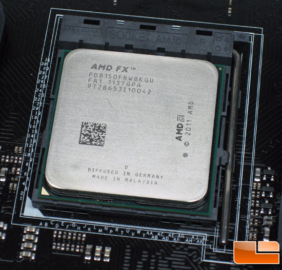
AMD FX Processors

AMD FX 8-Core Processor Black Edition and it’s unlocked for your overclocking 

pleasure. Experience unmatched multitasking and pure core performance with the industry’s first 32nm 8-core desktop processor. Get the speed you crave with AMD Turbo CORE Technology to push your core frequencies to the limit when you need it most. Go beyond the limits of maximum speed with easy-to-use AMD OverDrive™ and AMD Catalyst Control Center™ software suites. But the best part of all? You’ll get all this impressive performance at an unbelievable price. You’ll be asking yourself “what competition?” in no time.

AMD FX Processor Product Brief 


AMD FX Processors unlock maximum, unrestrained processing performance for extreme responsiveness you can see and feel.


Maximum Performance

  • The industry’s only 8-core desktop processor
  • Overclock with easy to use AMD Overdrive™ and AMD Catalyst Control Center™ software suites1
  • Supreme power available from virtually every core configuration - also available in 6- and
    4-core variants
  • Aggressive performance for mega-tasking and intensive applications like video editing and
    3D modeling

Innovative Architecture

  • The industry’s first and only native 8-core desktop processor for unmatched multitasking and pure core performance with all new “Bulldozer” architecture
  • New 32 nanometer die shrink designed to reduce leakage for improved efficiency, increased clock rate headroom and better thermals
  • Can deliver more cores and more performance without raising the power requirements

Industry Leading Price Per Performance

  • Unlocked processors allow the maximum tunable performance1
  • AMD Turbo CORE Technology dynamically adjusts performance to give you the best experience, no matter what you are doing
  • Get superior performance at a competitive price with unlocked technology

AMD FX 8-Core Processors

  • The industry’s first and only native 8-core desktop processor for unmatched multitasking and pure core performance with all-new “Bulldozer” architecture.
  • New 32 nanometer die shrink designed to reduce leakage for improved efficiency, increased clock rate headroom and better thermals.

AMD Turbo CORE Technology

  • The AMD FX Processors come equipped with AMD Turbo CORE Technology. AMD Turbo CORE Technology is a performance boosting technology that helps increase performance on the applications that need it the most.

New Instruction Capabilities

  • AVX 
    • Advanced Vector Extensions increase parallelism tailored for scientific and 3D applications that use heavy floating point calculations
  • FMA4 and XOP
    • Floating Point Vector Multiply -Accumulate  improves throughput and performance on many vector functions (integer and floating point)
  • AES
    • Advanced Encryption Standard noticeably increase performance on the latest encryption applications like TrueCrypt and benchmarks like PCMark

AMD Balanced Smart Cache

  • Shared L3 cache ( up to 8MB) 
    • Improved scheduling and pre-fetch capabilities
    • 64-ways (16-ways/sub-cache)
    • Increased data queue sizes
    • Coherency for 8-cores

AMD Wide Floating Point Accelerator

  • Shared FP Scheduler
  • Dual 128-bit Floating point engines – capable of teaming together for 256-bit AVX instructions or operating separately with each core.

HyperTransport™ Technology

  • One 16-bit link at up to 5600MT/s 
  • Up to 8.0GB/s HyperTransport™ I/O bandwidth; Up to 16GB/s in HyperTransport Generation 3.0 mode
  • Up to 37GB/s total delivered processor-to-system bandwidth (HyperTransport bus + memory bus)
Benefit: Quick access times to system I/O for better performance.

Integrated DRAM Controller with AMD Memory Optimizer Technology

  • A high-bandwidth, low-latency integrated memory controller 
  • Supports up to DDR3-1866
  • Supports new low voltage memories of 1.35V and 1.2V
  • Up to 29.9GB/s memory bandwidth for DDR3
  • New Pre-Fetcher improvements
  • Direct communications to each core in Dual-Core module (APIC registers in each core)
Benefit: Optimized memory controller to feed more cores

AMD Virtualization™ (AMD-V™) Technology with IOMMU

  • Silicon feature-set enhancements designed to improve the performance, reliability, and security of existing and future virtualization environments by allowing virtualized applications with direct and rapid access to their allocated memory.
  • IOMMU is an extension to AMD64 architecture to support address translation and access protection on DMA transfers
    • Security for User Level application and Virtual Machine guest operating system
      • Address translation and access control
      • Device isolation
      • Device assignment in virtualized systems
      • Security & trusted boot support
      • Unified interrupt management
Benefit: Helps virtualization software to run more securely and efficiently enabling a better experience when dealing with virtual systems

AMD PowerNow!™ Technology (Cool’n’Quiet™ Technology)

  • Enhanced power management features which automatically and instantaneously adjusts performance states and features based on processor performance requirements
  • C6 power state for cache flush, and voltage down individual core
  • CC6 power state allows all cores in C6 to power even lower
    • For quieter operation and reduced power requirements 
  • Separate memory controller power control
  • IO-based c-state interface
  • Works automatically without the need for drivers or BIOS enablement. 
  • Power can be switched on or off within a single clock cycle, saving energy with no impact to performance.
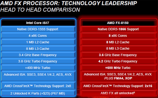
Below is the pic showing the technical comparison of the latest offerings from two Microprocessor titans AMD and Intel

Read More
Posted in | No comments
Newer Posts Older Posts Home
Subscribe to: Posts (Atom)

Popular Posts

  • Gigabyte's Wireless Laser Mouse -- ECO600
    Laser Mouse 12-month Battery. Energy Saving From Now On! GIGABYTE, a leading manufacturer of motherboards and graphics cards, is pleased to ...
  • AMD's A-Series Laptops are here, desktops in pipeline
    AMD has expanded its A-Series processor line with the first chips designed for desktops. The new chips join a lineup that includes seven mob...
  • Single-Layer Tin Could Go Beyond Graphene, Conducting Electricity with 100% Efficiency
    2D Tin Could Be Next Super Material, Say Theorists A single layer of tin atoms could be the world’s first material to conduct electricity wi...
  • Enterprise Resource Planning ( ERP )
    Enterprise Resource Planning (ERP) ERP denotes Enterprise Resource Planning that is a technique of using computer machinery to connect diver...
  • New lithium-ion battery design that’s 2,000 times more powerful, recharges 1,000 times faster
    Researchers at the University of Illinois at Urbana-Champaign have developed a new lithium-ion battery technology that is 2,000 times more p...
  • Holey Optochip First to Transfer One Trillion Bits of Information per Second Using the Power of Light developed by IBM
    IBM scientists today reported of a prototype optical chipset, dubbed “Holey Optochip”, that is the first parallel optical transceiver to tra...
  • CRM Solutions and Services
    CRM Solutions Customer Relationship Management (CRM) solutions help you to manage your customers more efficiently in an increasingly competi...
  • Apple and Microsoft aiming to eliminate the use of mouse...........
    The personal computer is a term that is used widely but yet not really defined. You may argue that it doesn't need to be defined as it i...
  • New discovery might lead to laptops powered through typing
    Everlasting batteries and self-powered portable electronics have come one step closer to reality, according to the results of new research b...
  • Fully Laser Integrated Photonics (FLIP) - A revolution in Computing Technology on the edge
    Fully Laser Integrated Photonics  (FLIP) may replace conventional electronics in a whole lot of computing and cut down computing's ever...

Blog Archive

  • ▼  2013 (4)
    • ▼  November (4)
      • New lithium-ion battery design that’s 2,000 times ...
      • Single-Layer Tin Could Go Beyond Graphene, Conduct...
      • Qualcomm Unleashes High-End Mobile Application Pro...
      • Synaptic Transistor Learns While It Computes
  • ►  2012 (4)
    • ►  March (1)
    • ►  February (2)
    • ►  January (1)
  • ►  2011 (37)
    • ►  October (2)
    • ►  September (1)
    • ►  August (5)
    • ►  July (12)
    • ►  June (5)
    • ►  May (12)
Powered by Blogger.

About Me

Unknown
View my complete profile